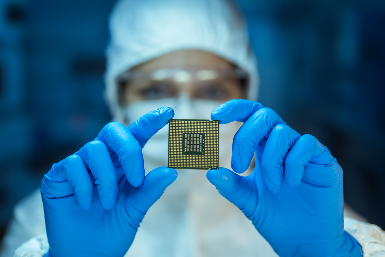
Few industry leaders have the breadth of knowledge Ray Zinn has achieved in semiconductors. Over his lifetime, the evolution of the technology has literally changed the world and employed countless millions upon millions. In this edition of his very popular Tough Things First podcast, Ray is joined by industry insider Robert Quinn to discuss the remarkable and revolutionary engineering history of the semiconductor.
Ray Zinn: Hello, everyone. Welcome to another Tough Things First podcast. I’m so delighted to be here today with a longtime friend from the industry, Robert Quinn. So how are you doing today Robert?
Robert Quinn: Doing great, Ray. How you doing?
Ray Zinn: We’re doing great. So it’s good to have you with us as we talk about how the industry has changed over the last 50 years. Robert, why don’t you tell us where you are, what’s going on with you and your career in the industry and then we’ll launch right into talking about how the industry has changed over the last 50 years.
Robert Quinn: Well, Ray, as you know, I’m somewhat of a LinkedIn semiconductor industry content provider for everybody.
Robert Quinn: It started about a year and a half ago. I started just adding content to LinkedIn about the semiconductor industry. It was part of my daily job to research the industry and find out what’s going on. And there was a guy named Gary Vee. He said, “Do something for others and ask for nothing in return.” And so I said to myself, “What can I do for others and ask for nothing in return?” I said, “Well, I’m spending the day researching and finding out information about the industry and I could just easily cliff note that information and share it on LinkedIn for others.” And before I knew it, I was adding a hundred people a day to my LinkedIn. I was getting phone calls from CEOs and leaders of billion dollar industries. And people were just ecstatic that I was making all these posts and talking about the semiconductor industry.
And lo and behold, here we are almost two years into this and I’m at over two million views per year on my LinkedIn and about 28,000 followers. So yeah, it’s been quite a ride. My former career was an engineer in semiconductor industry. I’ve been a field service engineer for over 20 years and I’ve traveled all over the world and I’ve been to almost all the fabs in the United States. And so it’s good to be able to talk about the industry and be able to speak with people about the industry. There’s just so much growth and so much going on right now, Ray.
Ray Zinn: Well, that’s great. Well, it’s good to have you with us today to talk about the industry, how it’s changed over the last 50 years. Next year, Robert, it will be my 50th year in the semiconductor industry. Can you believe that?
Robert Quinn: That’s awesome. That is incredible.
Ray Zinn: Yeah. So I started in 1963. The industry began, at least the part that I know, which is Fairchild, began in 1957. I joined in 1963 just six years later. And so I’ve seen the industry go from virtually a single transistor to starting my own company in 1978. Ran that for 37 years and then sold the company in 2015. And since then I’ve been writing and I’m on my fourth book now, and doing teaching, and just doing whatever I can to give back, like you said, to the industry. And so with that in mind, Robert, how do you see the industry’s changed over the last 50 years?
Robert Quinn: Oh gosh. I started in 2007 in Applied Materials and that was the time that the 200 millimeter Endura was coming in heavy. P-5000s were kind of phasing out at that timeframe and the Enduras were coming in really strong and the PVD tools you couldn’t make enough at that time. And then where it’s gone from this 200 millimeter and then went to 300 millimeter. I can’t really talk much about before the 200 millimeter phase, because I really wasn’t around for that very much, but where it’s gone from it from a tube transistor to a trillion transistors on a wafer right now is just absolutely amazing.
Robert Quinn: I was actually sitting down, speaking with a friend of mine last weekend and he was like, “So what do you? What are computer chips and why are computer chips so special?” And I tried to explain to him what is a transistor. Do you remember the transistor tubes that they used to have on the back of computers. Back in the ’50s and the ’60s they had these transistor tubes. Yeah. We fit a trillion transistors now on a single trip. And it’s amazing with the technology. We’re bringing this technology down to moving atoms where I’ve formally worked on a tool called atomic layer deposition. And we’re literally moving atoms on this equipment. And it’s amazing seeing the technology go from where we were at in the ’50s and ’60s to now we’re talking about doing two nanometers and three nanometers at full production. The technology scale has been absolutely just incredible to watch.
Ray Zinn: Well, when I started in ’63, we were on 10 millimeter wafers.
Robert Quinn: Wow. Wow.
Ray Zinn: And so we used light bulbs to expose the photo resist. And we didn’t talk about geometry. We didn’t talk about two nanometer or anything. We were just making single transistors. Planar of course. That was back in the day when Noise developed a planar technology. And so we were just making single transistors. It wasn’t until 1964 that we actually made the first integrated circuit. And I can remember that day very, very well. Everybody was just applauding and just hoop and hauling when we saw the first flip flop work. It was a flip flop. That’s what we made. And so we were all just jumping up and down so happy when we could get an integrated circuit made. And at the time we had just completed fab three at Fairchild on Westman road. And that was going to be what we called DIC, which is our digital integrated circuit fab.
Ray Zinn: So we had fab one, which made NPN transistors, and then fab two was PNP, and then fab three was DIC or digital integrated circuits. And, I was involved in making the first three tier tube furnace that we developed. I remember that Charlie Sporck, who at the time was the GM at Fairchild. He’s a very tall guy. He’s over six four. And he could reach that top tube, but the girls couldn’t. These little Filipino girls and so forth could not reach that top tube. And I had to build a ladder for them to climb up to reach that third tube. And so those were funny days as we were developing that three tube furnace.
Ray Zinn: It was a two inch tube actually. So we were moving into two inch wafers at the time and developing all the necessary processing hardware to do that. We had to make our own DI water plant. Actually, I worked on developing that water plant myself. And then we were trying to come up with a new design Epi Reactor. And I worked on that too, that the horizontal tube reactor, the first one we did. And, so we were developing all of our own equipment. Every single piece of equipment we were developing our ourselves, whether it be a seed grower for the crystals or whether it was Epi Reactors.
Ray Zinn: I remember developing the first ultrasonic bonder at the time. Because we were using the capillaries and gold wire, which we were called gold ball bonding, to connect the transistor to the lead wire on the package that we were using. It was just a three legged transistor. It had just basically just a three leaded part. And we were so excited to be able to do that and actually developed our own packages. The TOT50 was the first package that we developed on our own or maybe it’s called the TO50. Anyway, TO50, TO51 package. We actually built our own packages.
Ray Zinn: And so, back in those days, and in the early ’60s you had to develop all your own hardware, all the processing equipment. Everything was liquid etched and processed liquid wise. We didn’t use any gases except in the furnaces to diffuse the transistors. It’s gone from, let’s say 10 millimeter when I started, to now we’re on 300 millimeter wafers and might be even growing bigger. I remember 1964 or 5 that they doubted that we could even do Epi on anything larger than two inch. I remember on the chalkboard, we were actually doing the math models to show that you couldn’t get a uniform Epi layer over much over two inches. And so, it’s just all the things we had to learn and do and overcome. It was really exciting time for us as we were back in the early ’60s developing these early, early transistors.
Ray Zinn: That’s kind of my recollection of the very early days. The Silicon Valley, all way from the outskirts of San Jose to Sunnyvale was prune orchards and there was no buildings at all. It was just all orchards and had stoplights on Bayshore Freeway or on Highway 101. We actually had several stoplights and no overpasses at all. That’s the early days, Robert, of the very early 1960s in Silicon Valley.
Robert Quinn: I still have the hardest time trying to explain to people what we do. And I tell people, “Hey, we work on the machines that make computer chips.” And they still just don’t get it sometimes.
Ray Zinn: Well, it’s changed dramatically. We started outsourcing wafers to Europe and actually to Japan and Singapore and the early days of outsourcing as you would. And that took place in the early ’70s. That’s when we started really outsourcing, meaning doing wafer processing offshore because we had to get to the point where equipment was actually available from people like Applied Materials and others, Thermco, and these other companies that were making this equipment. As soon as it became commercially available, then we started outsourcing wafer fabrication. But up until then, all the fabbing was done basically in the US, mostly in Silicon Valley. That’s why they ended up calling it Silicon Valley because 80% of all the processing was done in Silicon Valley. But with outsourcing, then that began the move for every country in the world picking up the technology and developing wafer and processing wafers. That’s what started the outsourcing, was when all that equipment became available commercially for companies to install and build fabs outside the US because it became very, very expensive.
Ray Zinn: I can remember back in the mid ’70s when Intel was really starting to get rolling. They were saying that it was going to cost a hundred million dollars to put a fab together. And we laugh at that now, because we’re talking a hundred times that maybe, a hundred billion to put in a fab. The alignment tools just to make the image, the circuitry on the wafer, used to cost less than $20,000. And now they cost over 10 million dollars for an imaging tool. You know what I’m talking about, Robert. You can reflect on the difference in pricing. A three tube furnace used to cost us less than $60,000 to build back in the early ’60s.
Robert Quinn: Wow.
Ray Zinn: And and as I said, the alignment tools to actually image the wafer cost less than $20,000.
Robert Quinn: Wow.
Ray Zinn: And I remember when I developed the wafer stepper back in ’74 at Electromask, I charged TI $800,000 for each unit. And that was the most expensive piece of equipment that was ever built for semiconductors was back in 1974, ’75 when I developed the stepper. And that was a $800,000. Compare that to the alignment tools that we were using back in the early ’60s. It cost less than $10,000 or $20,000. We used to use a lathe, a XY axis, to align it. We did it with the little knobs to align from one image to the other. Of course, we didn’t have more than three or four layers back in those days. And now we got hundreds of layers now that we image.
Robert Quinn: Yeah. I can recall walk walking through a couple of the different fabs that I’ve worked in and the fabs were billion dollar rows. They said go down to billion dollar row and you’ll take a left because everybody knew where billion dollar row was, because that was a billion dollars of equipment on a single bay. And it’s incredible how the accumulation of money, the cost of running these fabs and buying the equipment today is just absolutely incredible. They’re saying now that the new EUV tool is up to 200 million dollars for a single tool. It’s absolutely just incredible to think about. Nowadays we have Samsung coming in with, I believe it was 17 billion dollars. TSMC is coming in with, I thought it was around 13 billion, don’t quote me on that. But TSN Intel coming in Ohio, the $20 billion fab. And these are all just starts. And I’m sure they’ll continue to add to all these fabs as well. These are incredibly expensive and the cost of equipment is getting higher and higher. It’s incredible to watch.
Ray Zinn: Well, I started Micrel in 1978, but in ’81 I bought my first fab as a used fab over on Pastoria in Sunnyvale. And it was a used fab it was three inch, but I only paid 1.6 million dollars for an entire fab with the processing tools, the technology all in place, including the operators and the building. I paid 1.6 million for the whole fab. Okay. And that was in 1981.
Robert Quinn: Yeah.
Ray Zinn: And so today, as you pointed out, a fab now can easily cost you 10 billion or more, 20 billion, 30 billion.
Robert Quinn: Right.
Ray Zinn: The stepper that I did in 1975 was 435 nanometer technology on eight inch wafers cost $800,000. Now for a 300 millimeter stage doing, I understand at seven nanometer, is 12 million dollars or something like that dollars for a single stepper. And now you said, now it may cost, how much did you say? 200 million for a DUV?
Robert Quinn: Yes. I believe they’re saying the top end scale is around 200 million, I believe. So they were saying it started at 150 million about a year ago, and I think they’re saying that a top end scale for EUV is close to 200 million. So-
Ray Zinn: Well, let’s end it here so we don’t jump into where we see it going in the next five years. So I hope you guys, all you listeners enjoyed our podcast today. And I’m so delighted to have Robert with me. And what’s the name of your podcast?
Robert Quinn: Don’t have a podcast. I’m on LinkedIn. Just follow me on LinkedIn. I do webinars every month and I interview CEOs and leaders in the semiconductor industry. And so we have some really good content coming out with some great leaders. Just recently had a show with Ray and we got quite a great lineup coming up in the next three months. So…
Ray Zinn: You can be followed on Robert Quinn on LinkedIn?
Robert Quinn: Yes. Yeah.
Ray Zinn: Okay.
Robert Quinn: Robert Quinn at LinkedIn.
Ray Zinn: Super. And please read my books, Tough Things first. It’s been out for last seven years. You can read that. That’s still a textbook in the industry. It’s also textbook at several universities. It’s how to run a company. That’s the name on my book, Tough Things First, is how to run a company. And then I’ve written two more since then, Zen of Zinn 1, Zen of Zinn 2, Zen of Zinn 3 is going to come out sometime in July and would like invite you to follow me on LinkedIn, Twitter, and Facebook. And thanks again, Robert for joining us. And we’ll continue on with our next podcast.
Robert Quinn: Thank you, Ray. And I’ve been enjoying your books as well. They’re very good. Thank you so much.
Ray Zinn: Thanks for the review.
